
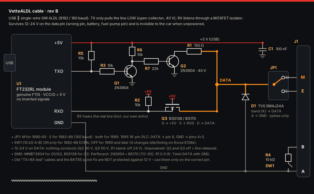
The problem with most DIY cables
The GM 8192 baud ALDL line is a single open-collector wire: inside the ECM (and CCM, ABS …) a ~10 kΩ resistor pulls it to +5 V and each module pulls it low with a transistor to send a 0 bit. Idle = high. Everybody may only pull low; nobody may drive it high.
The popular "$20 cable" ties the FT232R's TXD and RXD together straight onto pin M. TXD is a push-pull output that drives the line high whenever it idles, so every 0 bit from the ECM becomes a fight between the ECM's transistor and the FTDI output. Depending on the parts the resulting "low" sits at 0.5–1.5 V – right at the receiver thresholds – and you get framing errors and garbage, worse when the CCM chatters. The same cable also stresses the ECM output.
Two more classic traps:
- FT_Prog "Invert TXD/RXD" – correct only for RS-232 (DB9) adapters that have an inverting transceiver. On a TTL FT232R board it makes TX idle low (holding the whole car bus down – the CCM then logs code 41) and RX reads inverted data.
- 3.3 V boards / VCCIO jumper on 3.3 V – the line is 5 V; use 5 V I/O.
Recommended design (rev B)
| Ref | Part | Why |
|---|---|---|
| U1 | Genuine FTDI FT232RL breakout, VCCIO jumper = 5 V (or FTDI TTL-232R-5V) | USB ⇄ TTL UART, 5 V logic, no driver sabotage |
| Q1 | 2N3904 NPN (SMD MMBT3904) | inverter: TXD idle HIGH → Q1 on → Q2 off |
| Q2 | 2N3904 NPN, 40 V (SMD MMBT3904, PN2222A fits) | open-collector line driver – only ever pulls the line LOW, like every GM module |
| Q3 | BSS138 N-MOSFET 50 V (SOT-23) or BS170 (TO-92) | RX isolator: gate on +5 V, source → RXD, drain → DATA |
| R1 | 150 Ω, 0.5 W | series resistor of Q2 |
| R2 | 10 kΩ RXD → +5 V | RX idle level (bench, car off) |
| R3 | 10 kΩ | Q1 base |
| R4 + SW1 | 10 kΩ + switch between A and B | diagnostic enable for 1982–88 (160 baud) ECMs only, OFF for 1989+ |
| R5 | 10 kΩ TXD → +5 V | TXD high while the FTDI boots or is unplugged → line released |
| R6 | 10 kΩ Q1 collector → +5 V | base drive for Q2 |
| R7 | 22 kΩ | Q2 base – deliberately high, limits short-circuit current |
| C1 | 100 nF | 5 V decoupling |
| D1 | TVS SMAJ24A, unidirectional – band (cathode) on DATA, anode on GND | spikes only (ESD, ignition); does not conduct up to 24 V |
| JP1 | 3-way selector | M (1990–95), E (1982–88), E+M (1989) |
| J1 | GM 12-pin ALDL plug | 1995: 16-pin DLC, data pin 9, GND 4+5 |
How it works
- TX – TXD idles HIGH, Q1 conducts, Q2 is off: the line is released. A 0 bit (TXD LOW) turns Q1 off, R6+R7 drive Q2's base and Q2 pulls DATA low through R1. Two inversions = the same logic as the FTDI TX, so no FT_Prog inversion is used. Low level ≈ 0.1 V + R1 × bus current (≈0.2–0.4 V with a 2–10 kΩ bus pull-up).
Polarity (identical in rev A and rev B – both are non-inverting):
UART state TXD rev A: 74LVC1G07 output rev B: Q1 rev B: Q2 DATA line idle / stop bit / 1 bit HIGH high-Z (released) on off HIGH (bus pull-up) start bit / 0 bit LOW pulls low off on LOW A single transistor or open-drain stage on its own would invert (base HIGH → line LOW); the 74LVC1G07 contains buffer + open drain (non-inverting, the small diamond on its symbol marks the open-drain output, it is not an inversion bubble), and rev B uses Q1 to cancel Q2's inversion. An inverted stage would hold the bus LOW whenever the UART idles – see "Why polarity matters".
- RX – Q3 is the classic MOSFET level shifter. When anything pulls DATA low, Q3's body diode and then its channel pull RXD low; when DATA is high (5 V or even 24 V), Q3 is off and R2 holds RXD at 5 V. RXD therefore only ever sees 0–5 V, and it sees the real line, so every byte we transmit comes back (echo) and VetteALDL checks it byte by byte.
- Unpowered – with the USB unplugged Q1/Q2 have no base drive and Q3's gate is at 0 V, so the cable is truly invisible to the car (rev A still loaded the bus through R3 and the RXD input).
- Bench loopback works without the car: Q2 pulls the open DATA wire low, Q3 passes it to RXD.
Why polarity matters
A UART idles HIGH (mark) and a byte starts with a LOW start bit; the ALDL line also idles HIGH and modules pull it LOW. So the line must follow TXD directly. If one stage inverted:
- the bus would be held LOW all the time the app is not sending – the CCM loses the ECM (code 41), the dash loses ECM data and nobody can talk;
- every byte would reach the car inverted (start bit HIGH = no start bit), so nothing is understood;
- "fixing" it with FT_Prog "Invert TXD" is fragile: before the FTDI loads its EEPROM (plug-in, USB reset, unplugged laptop) the line would be pulled LOW again.
The connection debugger catches this on the bench (step 2: the line is stuck low / echo inverted) and from the EEPROM (step 1: "inverted lines").
What happens if 12 V (or more) reaches the data pin
The ECM itself never puts 12 V on the ALDL data line (see below), but a wrong pin, an off-by-one plug, the fuel-pump test pin G on 1984–89 cars, pin 16 (battery) on the 16-pin DLC or a harness fault can.
| Voltage on DATA | Rev B | Rev A (74LVC1G07 + clamp) |
|---|---|---|
| 12–16 V, idle | nothing conducts (Q2 40 V, Q3 50 V, D1 24 V stand-off); R2 keeps RXD at 5 V | the clamp diode takes amps from a low-impedance source and burns; U2 (abs. max 6.5 V) gets ~55 mA through R1 and dies |
| 12–16 V while transmitting | Q2 current limited by its base drive to ~15–40 mA; RX sees the line stuck HIGH → echo error → the app stops sending | as above |
| 24 V (jump start) | nothing conducts (D1 stand-off 24 V) | as above |
| spikes > 27 V | D1 clamps (≤ 39 V at 10 A, below Q2's 40 V) | clamp at ~6–7 V |
Old "TX+RX tied" cables and the BAT85 quick fix below are not protected: 12 V would be forced into the FTDI TX pin. Use them only on the correct pin.
What the data line looks like inside the car's modules
The GM 8192 baud ALDL line (pin M, 1990–95; pin 9 on the 1995 16-pin DLC) is not the European ISO 9141 K-line/L-line (12 V, used e.g. by Opel/Vauxhall – the Tech 1 has a separate KW2000 cartridge for that). It is a single bidirectional wire:
- each module (ECM, CCM, ABS, SIR, climate) has an open-collector (NPN) output that pulls the wire to ground to send a 0 bit and releases it for a 1 bit;
- the wire is pulled up to the ECM's regulated 5 V through a resistor (order of 10 kΩ; the exact value for the 1227727 is not documented in our sources – measure it if you need it, see below);
- every module also listens on the same wire (a comparator/transistor input), so each hears its own transmission – that is why the bus works as a "wired-AND" and why our cable must only pull low.
The 160 baud line (pin E, 1982–88) is also a 5 V open-collector output of the ECM, but it only transmits (pulses) when the 10 kΩ A–B resistor is present. Some other GM systems of that era used a 12 V serial line (the Tech 1 self-test even has "LOW SPEED 12 V SERIAL DATA"); rev B works with those too because Q2 and Q3 tolerate 40/50 V.
To estimate the pull-up of your car: ignition ON, engine off, measure DATA (M) to ground (A) with the cable unplugged – about 5 V (the CCM traffic makes it flicker). Then put a 10 kΩ resistor from M to A and measure again: R_pullup ≈ 10 kΩ × (5 V − V) / V. Keep it short – while loaded the CCM may lose the ECM and store code 41, which you can clear afterwards.
History: rev A
Rev A used a 74LVC1G07 open-drain buffer, 4.7 kΩ into RX, a 47 kΩ pull-up and a clamp diode on the line. Drawings before 2026-09-26 showed that diode reversed (anode on DATA = the bus held at ~0.6 V) and as a 5.0 V TVS; both are fixed, and rev B replaces the whole front end because rev A does not survive 12 V on the data pin.
Quick fix for an existing TX+RX-tied cable
Cut TX, insert a Schottky diode (BAT85/1N5817): band (cathode) toward TXD, anode toward the ALDL line; put 4.7 kΩ in series with RX; 5 V board; all FT_Prog inversions OFF.
Not protected against 12 V on the data pin (the diode would forward 12 V into the FTDI TX) – use it only on the correct pin and build rev B for anything permanent.
12-pin ALDL (car socket, seen from the cabin)
 F  E  D  C  B  A        A = ground          B = diagnostic enable (ECM)
 G  H  J  K  L  M        E = 160 baud data (1982–89)   M = 8192 data (1990–95)
                         G–A = dash diagnostics 1990–93 (NEVER on 1984–89: G = fuel pump)
Test procedure
- Bench: VetteALDL → Connection debugger step 1 (PC & driver) and 2 (loopback) – must be 100 % clean.
- Car, ignition OFF: step 3 – the data wire must not be on a ground pin.
- Ignition ON: step 4 – CCM traffic visible, ECM answers.
- Anything red → Sessions & support → Create support bundle.